PORTFOLIO:
Circuit 6: Pattern Matcher (Simon Says) — EPROM-driven breadboard
Design narrative
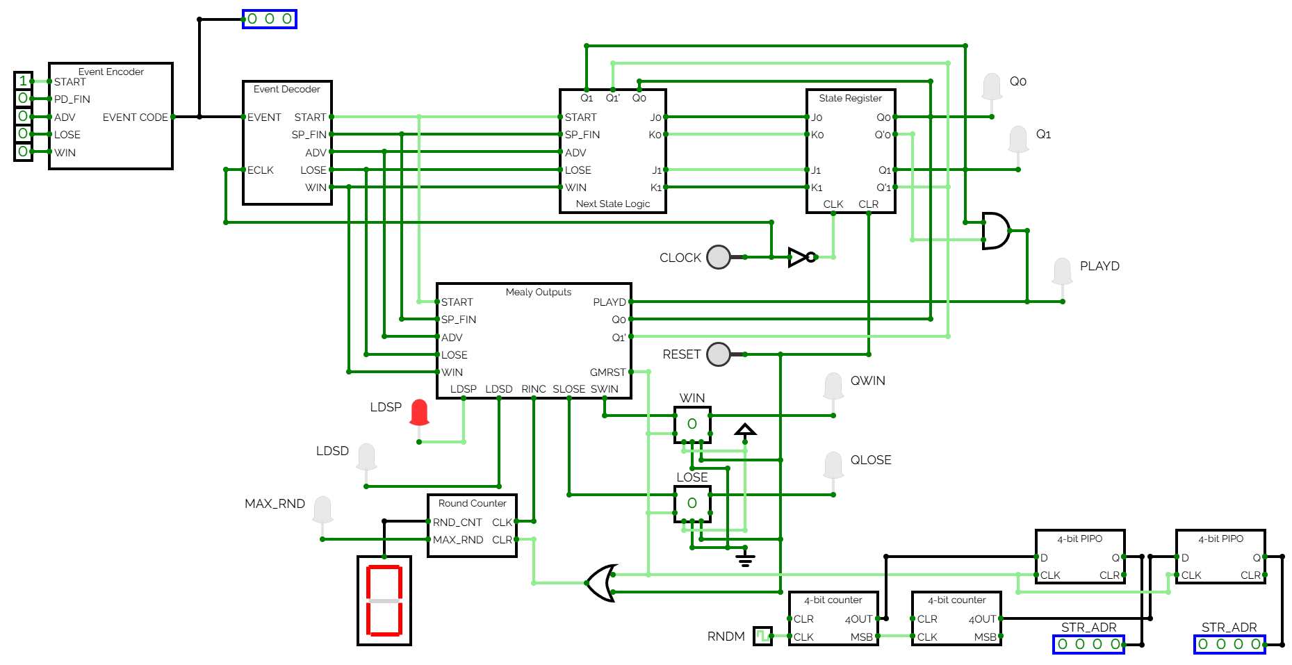
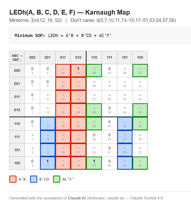
Circuit 6 is the Pattern Matcher for my Simon Says design project, breadboarded as a standalone demo of the EPROM-driven pattern-comparison logic. A 27C64 EPROM holds a value sequence; a 74191 counter walks through it one address per correct keypress; a 7485 magnitude comparator checks each press against the expected value stored at the current address; and a small 2-state FSM handles the press-evaluation timing.
The comparator choice came out of an encoding pivot. I’d originally planned one-hot for both BTN and EPROM_OUT, and I was considering a few methods for the comparison — an AND-OR tree pairing each button bit with its matching EPROM bit, a small decoder pattern, a couple of others. Right before Agnes and I programmed the EPROM, we switched the input from discrete pushbuttons to a keypad, and that decision did the comparator choice for me. The keypad gives four arbitrary 4-bit codes for the four values (0, 1, 4, and 5 — the keys we picked), so the inputs weren’t one-hot anymore. Once they weren’t one-hot, a 7485 4-bit magnitude comparator’s A=B output became the obvious move. One chip, no gate tree, equality is equality. The EPROM bytes were written using the same encoding so the comparator sees a clean match when the player presses the expected value. The keypad also handles two things I’d been planning to build separately: it prevents simultaneous presses (only one key is encoded at a time), and it provides a data-available pin that goes high while a key is held — so the FSM doesn’t need a press-detect OR-tree across the four button lines.
The PM owns its own state machine for the press-evaluation timing. Rather than wiring raw button signals through to the rest of the system and asking it to figure out when a press has been evaluated, PM runs a 2-state FSM (LISN ↔ CHEK). LISN is “waiting for a press.” A clean touch transitions to CHEK. The release back to LISN is where evaluation fires — INC_PM on a good match, LOSE_FLAG on a bad one. Detecting on the release rather than the touch means a held button doesn’t repeat-fire across clock cycles.
The MATCH latch is the trick that makes the release timing work. The live comparator output is valid only while a button is held, because after release the keypad bus drops and COMP goes low. So I clock-enabled a JK flip-flop on the LISN → CHEK transition, capturing the comparator value at the moment of press touch and holding it through CHEK. By the time the release fires, MATCH still reflects what the comparator saw at touch. JK’s J=K=0 hold-for-free semantic does the work cleanly — when MATCH_LD_EN is low (which is most of the time), the flip-flop holds whatever value it last captured.
The standalone version is a minimum-viable demo of the press-evaluation chain: a reset button, an EPROM, a counter, the comparator, the MATCH latch, and the 2-state FSM. Correct press advances the counter; wrong press lights the LOSE LED and holds. There’s no round counter and no round-complete logic in this build — those layers (along with multi-button rejection and a response timer) live in the integrated Simon Says machine, not here.
Inputs, outputs, and behavior
Inputs
- BTN[3:0] — 4-bit keypad output through a 7414 Schmitt inverter chain. The four playable values map to keypad codes 0, 1, 4, and 5.
- Data — the keypad encoder’s data-available pin. High while a key is held. The PM-FSM uses this as the “press is active” signal; no four-input OR across the BTN lines required.
- EPROM_OUT[3:0] — data lines D[3:0] from the 27C64. D[7:4] are unused. The byte at the current pm_counter address holds the 4-bit code for the value expected at that step.
- LDPM (RESET) — pushbutton: asynchronously loads pm_counter to 1 and clears the PM-FSM state register to LISN. Used to start a new run.
- CLK — LM555 free-running clock, ~1.5 Hz at the demo configuration. Drives the PM-FSM state register and the MATCH latch.
Outputs
- INC_PM — Mealy pulse on CHEK → LISN release with MATCH = 1. Increments pm_counter to the next address.
- LOSE_FLAG — Mealy pulse on CHEK → LISN release with MATCH = 0. Drives the LOSE LED.
- step_counter[3:0] — the 4-bit counter, also driving EPROM ADDR[3:0]. Surfaced on four LEDs so the current step is visible.
- MATCH — latched comparator value, on an LED so the player can see “the press was registered as correct” while the button is held, before the release event fires.
Behavior
- Start a run: press RESET. pm_counter loads to 1, PM-FSM state clears to LISN.
- Correct press: on the press touch, the PM-FSM transitions LISN → CHEK and the MATCH latch captures the comparator’s “match” value (high). The MATCH LED lights. On release, the FSM transitions CHEK → LISN and INC_PM pulses, advancing pm_counter to the next address.
- Wrong press: the MATCH latch captures “no match” (low) on the press touch; MATCH LED stays dark through the hold. On release, the FSM transitions CHEK → LISN and LOSE_FLAG pulses, lighting the LOSE LED. pm_counter holds.
- Held button: the FSM holds in CHEK as long as a button is pressed, so a held button doesn’t repeat-fire its event. The event fires exactly once on the release edge.
- Reset: pressing RESET at any point reloads pm_counter to 1 and forces the FSM back to LISN.
Boolean expressions and tables
PM-FSM state encoding (single state bit):
| State | Bit | Meaning                                     |
|-------|-----|---------------------------------------------|
| LISN  |  0  | waiting for a press                         |
| CHEK  |  1  | press held, MATCH latched, ready to evaluate|
State transition table (Mealy pulses fire on the listed transition):
| From | Condition                  | To   | Mealy pulses |
|------|----------------------------|------|--------------|
| LISN | Data                | CHEK | MATCH_LD_EN  |
| LISN | else                       | LISN | —            |
| CHEK | Data' · MATCH       | LISN | INC_PM       |
| CHEK | Data' · MATCH'      | LISN | LOSE_FLAG    |
| CHEK | else (button held)         | CHEK | —            |
Final equations (state register is one JK flip-flop, encoded LISN = 0 and CHEK = 1):
Comparator (7485, 4-bit equality):
  COMP = (BTN[3:0] == EPROM_OUT[3:0])      (taken from the A=B output)

MATCH latch (JK-FF, clock-enabled on the LISN → CHEK transition):
  MATCH_LD_EN = LISN · Data
  J(MATCH)    = MATCH_LD_EN · COMP
  K(MATCH)    = MATCH_LD_EN · COMP'

PM-FSM next-state (JK-FF, J=K=0 holds):
  J(state) = Data
  K(state) = Data'

Mealy outputs (one-cycle pulses on the CHEK → LISN transition):
  INC_PM    = CHEK · Data' · MATCH
  LOSE_FLAG = CHEK · Data' · MATCH'
Acknowledgment
Claude Opus 4.X (Anthropic) served as my thinking partner for the design and presentation of this project. It helped me brainstorm, organize my working notes, and draft the prose, tables, and diagrams on this page at my direction. All design decisions were mine, and all Boolean minimization and schematic work were done by hand or with purpose-built tools — not by Claude. I own the final work.
References
[1] A. J. Pasquale, Digital Systems. Self-published, rev. 2 Dec. 2025. Referenced throughout.
Circuit 7: Game Controller FSM (Simon Says) — CircuitVerse simulation
Open the CircuitVerse simulation →
Design narrative
Circuit 7 is a Game Controller — the finite state machine for my Simon Says design project. Two state bits track three named states (IDLE — in between games, PLAY — showing the pattern to the player, USER — the player’s turn). Two Moore outputs decode the current state for the rest of the system. Six Mealy outputs pulse on transitions to load counters, set the win/lose latches, and trigger a game reset. The FSM sees a 3-bit event code from a priority-encoder front-end.
The first pass had six states — IDLE, PLAY, CHEK, USER, WIN, LOSE — and the FSM took nine raw input signals plus three state bits. LogicAid Petrick scored that at 185 input cost / 44 gate cost. With a 7400-series kit and only 2-input gates, that was way over the budget for a hand-built breadboard. I had to compress.
Two compression passes brought it way down. I merged states that did the same thing, offloaded the press-counting into the Pattern Matcher subsystem, and consolidated duplicate outputs. Six states became three (plus a fourth unused-code recovery row, BLNK). 81 input / 21 gate — a 56% / 52% reduction from the first pass.
For the state assignment I tested three classes for {IDLE, PLAY, USER, BLNK} through LogicAid. Class A — 00, 01, 11, 10 — won on hot-path single-bit-flip: IDLE→PLAY flips just Q1, PLAY→USER flips just Q0, and only the rare game-over path flips both bits. Around the same time I realized this FSM mostly holds. In almost every state·event combination the state doesn’t change. D flip-flops have to compute the held value explicitly for every hold path; JK flip-flops get hold for free with J=K=0. Switching to JK dropped the cost to 67/18, all of it in next-state logic.
The most interesting part was BLNK. Since BLNK isn’t reachable from any of IDLE, PLAY, or USER under any event, I marked its row “don’t-care” in the state table — letting the minimizer treat those outputs however gives the smallest cover. The headline win: USERD collapsed from a 1-gate AND (Q0·Q1) to a direct wire from Q0, because once BLNK is off the table, Q0=1 unambiguously means USER. Cost dropped to 57/17. But “don’t-care” cuts both ways — Petrick happily dropped the Q1′ term from K(Q0), which I’d been counting on for automatic recovery if a glitch ever did land in BLNK. Without that term, BLNK turns into a soft trap on some events. So I added Q1′ back manually as a single OR input. One extra gate buys guaranteed BLNK → IDLE recovery in one clock, regardless of event. Final cost: 58 input / 18 gate. Down 69% / 59% from the original six-state design.
The FSM proper — state register plus next-state logic — fits on a sub-board with six chips: one 74112 for the two JK flip-flops, three 7408s for the ANDs, one 7432 for the ORs, and a 7404 for the inverters that flip the three event bits to their complements. Three event lines and the clock come onto the board; four state outputs — Q0, Q0′, Q1, Q1′ — come off. The Moore decoders, Mealy pulses, encoder front-end, event register, round counter, and random start-address generator all live in the surrounding region of the board, alongside this sub-board.
Detailed reference manual
Full state encoding, event codes, output table, round counter and random start-address subsystem documentation, and the test-procedure walkthrough for the CircuitVerse simulation:
Inputs, outputs, and behavior
Inputs
- E0, E1, E2 — 3-bit event code from the priority-encoder front-end (MSB first). Five named events:
START(000),PD_FIN(001),LOSE(010),ADV(100),WIN(101). - CLK — clock. The event register latches on the rising edge; the state register samples on the falling edge (two-phase arrangement keeps multi-bit event transitions from reaching the FSM mid-update in the CircuitVerse simulation).
- RESET — asynchronous clear. Forces the state register to IDLE (00) and clears the WIN and LOSE latches and the round counter on the way down.
Outputs
Moore (state-only level signals):
- PLAYD — high in PLAY only. Drives the Pattern Display enable and the color LED bank.
- USERD — high in USER only. Drives the Pattern Matcher enable and the EPROM ADDR mux select.
Mealy (one-clock pulses on transitions):
- LDPD — parallel-load the Pattern Display step counter to the round’s start address. Fires on START·IDLE and ADV·USER.
- LDPM — parallel-load the Pattern Matcher’s user-turn counter at the start of the player’s turn. Fires on PD_FIN·PLAY.
- RINC — increment the round counter on a successful round. Fires on ADV·USER.
- SLOSE — set the LOSE latch on a wrong color or timeout. Fires on LOSE·USER.
- SWIN — set the WIN latch on the final-round completion. Fires on WIN·USER.
- GMRST — game reset. Clears the WIN and LOSE latches and the round counter at game start. Fires on START·IDLE.
Behavior
- IDLE → PLAY: START fires GMRST (clearing the end-game latches and the round counter) and LDPD (loading the Pattern Display from the random start address). The machine begins showing the sequence.
- PLAY → USER: PD_FIN fires once the Pattern Display has finished playing the round’s sequence. LDPM loads the Pattern Matcher’s user-turn counter; the player’s turn begins.
- USER → PLAY: ADV fires after a successful round with more rounds remaining. RINC increments the round counter and LDPD re-loads the Pattern Display for the next, longer sequence.
- USER → IDLE: either LOSE (wrong color or response-timer expiry) or WIN (final round complete) drops the FSM back to IDLE. SLOSE or SWIN sets the corresponding end-game latch.
- BLNK recovery: the unused 4th 2-bit code (Q0 Q1 = 10) is unreachable in normal clocked operation, but the manual Q1′ insurance term in K(Q0) guarantees that any glitch into BLNK returns to IDLE on the next clock edge regardless of event.
Boolean expressions and tables
State encoding (Q0 = MSB, Q1 = LSB):
| State | Q0 | Q1 | Meaning                                          |
|-------|----|----|--------------------------------------------------|
| IDLE  |  0 |  0 | between games — waits for START                  |
| PLAY  |  0 |  1 | Pattern Display playing the round’s sequence     |
| USER  |  1 |  1 | user pressing color buttons                      |
| BLNK  |  1 |  0 | unreachable in normal operation — recovery row   |
State transition table (Mealy pulses fire on the listed transition):
| From | Event   | To   | Mealy pulses     |
|------|---------|------|------------------|
| IDLE | START   | PLAY | LDPD, GMRST      |
| IDLE | else    | IDLE | —                |
| PLAY | PD_FIN  | USER | LDPM             |
| PLAY | else    | PLAY | —                |
| USER | ADV     | PLAY | LDPD, RINC       |
| USER | LOSE    | IDLE | SLOSE            |
| USER | WIN     | IDLE | SWIN             |
| USER | else    | USER | —                |
| BLNK | any     | IDLE | —                |
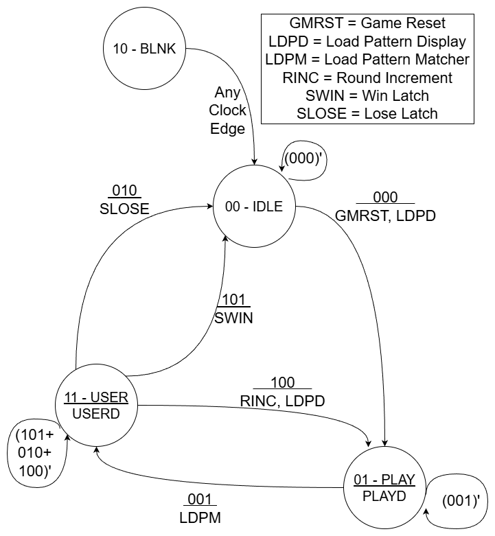
Final equations after the architecture sweep, Class A encoding, JK flip-flop pivot, BLNK don’t-care, and the manual Q1′ insurance term — 58 input cost / 18 gate cost from LogicAid Petrick:
Next-state logic:
  J(Q0) = PD_FIN · Q1
  K(Q0) = LOSE + ADV + WIN + Q1'           (Q1' = BLNK recovery insurance)
  J(Q1) = START
  K(Q1) = (LOSE + WIN) · Q0

Moore outputs:
  PLAYD = Q0' · Q1
  USERD = Q0                               (direct wire from the state bit)

Mealy outputs:
  GMRST = START · Q1'
  RINC  = ADV   · Q0
  SLOSE = LOSE  · Q0
  SWIN  = WIN   · Q0
  LDPM  = PD_FIN · PLAYD
  LDPD  = GMRST + RINC                     (shared subexpressions across LDPD’s two terms)
Acknowledgment
Claude Opus 4.X (Anthropic) served as my thinking partner for the design and presentation of this project. It helped me brainstorm, organize my working notes, and draft the prose, tables, and diagrams on this page at my direction. All design decisions were mine, and all Boolean minimization and schematic work were done by hand or with purpose-built tools — not by Claude. I own the final work.
References
[1] A. J. Pasquale, Digital Systems. Self-published, rev. 2 Dec. 2025. Referenced throughout.
Circuit 8: Volleyball Lineup Tracker — CircuitVerse simulation
Open the CircuitVerse simulation →
Design narrative
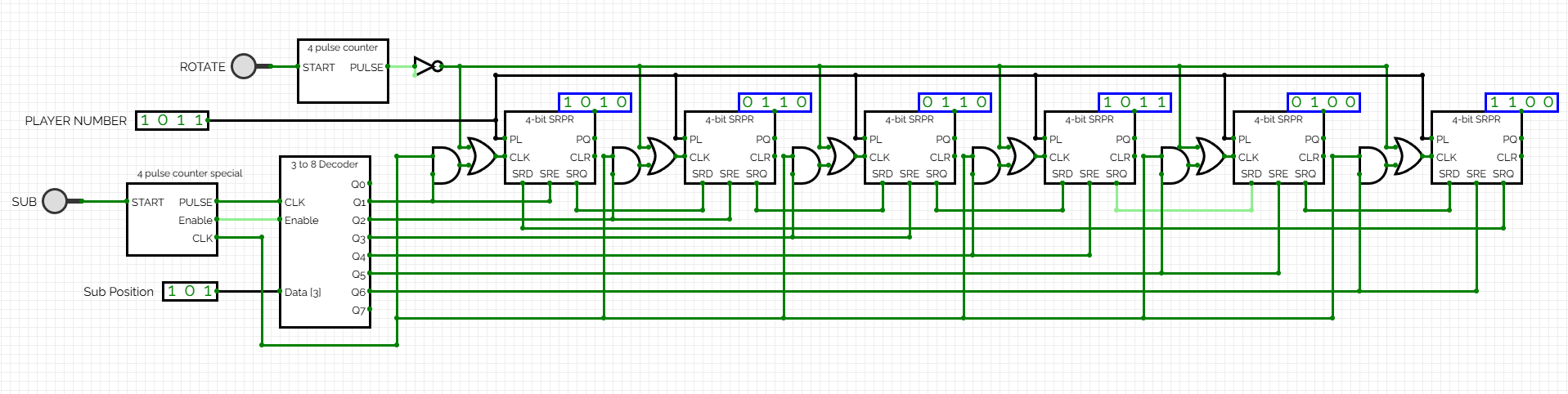
Circuit 8 is a volleyball lineup tracker, built on CircuitVerse. Six 4-bit register cells model the six court positions, and the whole design is a serial-chain shift register: each cell is linked head-to-tail to its neighbor by a single-bit serial wire, and the chain closes back on itself so the lineup is a ring. Two buttons drive it. ROTATE advances every player one court position; the cycle wraps 6 → 1, so P6’s player becomes the new server at P1, the old server moves on to P2, and so on around the ring. SUB loads a single new player at a selected court position from the 4-bit DATA bus, addressed by the 3-bit ADDR bus — the substitution operation.
I went with the serial-chain pattern over a parallel-rotation network because the wiring economy is significant: six single-bit inter-cell links instead of twenty-four parallel wires for the rotation path. The trade-off is that one position-rotation now takes four clock pulses (one per bit of a 4-bit jersey number) instead of one. The ROTATE button hides that under the hood — a small counter (Counter A, three D-FFs) fires a 4-pulse burst of the fastclock to all six cells in parallel, so one click is one full position rotation. From the user’s side it’s still one click per side-out; from the schematic’s side every cell is doing the simplest possible thing on each clock, just shifting one bit.
Substitution is the other operation. The SUB button arms the same 4-pulse Counter A I built for ROTATE — reused as-is, even though SUB only needs one timed pulse, because building a separate counter for the sake of trimming three unused edges wasn’t worth the gate count. Paired with the counter is a control flip-flop that drops LOW on SUB press, asserting the 3-to-8 decoder’s active-low enable; ADDR (3 bits) picks one of the six positions, the decoder pulls that cell’s SRE low into LOAD mode, and a CLK pulse fires out to all six cells in parallel. Per-cell AND gates with each cell’s SRE mean only the addressed cell (SRE low) actually sees the rising edge — that cell parallel-loads from DATA, the other five hold. At the end of the sequence the control FF resets HIGH, the decoder turns off, all six cells return to shift-mode default. Decoder enable was wired active-low specifically because the control FF naturally sits HIGH at rest — the polarity matched the natural quiescent state, no inverter needed.
Each cell is an SRPR — a 4-bit Shift-Right PIPO register I built as a reusable subcircuit in earlier work. It only shifts right; building exactly the register I needed saved a control pin and a chunk of logic both inside the subcircuit and outside it (no shift-left path means no left-vs-right select MUX, no extra control wiring, and no second serial-in/out pair). The pins are PL (4-bit parallel-load input), PQ (4-bit output), CLK, CLR, SRL (serial-in), SRQ (serial-out), and SRE (mode select — HIGH selects shift-right on the next clock, LOW selects parallel-load). Inside the subcircuit, each bit’s D input comes through a 2-to-1 MUX that picks between the SRL path and the corresponding PL path under SRE control. C8 instantiates the SRPR six times for the lineup cells.
The chain closes at the top — cell P6’s SRQ feeds cell P1’s SRL, so the bit that falls off the right end of P6 enters the left end of P1 on the next clock. Over four clocks the full 4-bit jersey number transfers from P6 into P1 and the whole lineup advances one position around the ring. The cyclic property falls out of the loop closure: six ROTATE clicks (twenty-four underlying clock pulses) returns the lineup to its starting configuration — the cleanest verification check on the wiring.
Inputs, outputs, and behavior
Inputs
- DATA[3:0] — 4-bit shared parallel-load data bus. The new jersey number for a substitution (0–15).
- ADDR[2:0] — 3-bit court position select for substitution. Codes 001–110 are valid (positions P1–P6); 000 and 111 are unused.
- ROTATE — momentary button. Each click arms Counter A, which fires a 4-pulse clock burst to all six cells. Lineup advances one position around the ring.
- SUB — momentary button. Each click arms Counter A (reused) and the control FF, briefly enables the decoder, and emits clock pulses to all six cells in parallel; only the addressed cell’s gated CLK actually fires, so only that cell parallel-loads.
- CLK — free-running fast clock. Shared by the counter and the rest of the timing.
Outputs
- P1[3:0] through P6[3:0] — the 4-bit jersey number currently at each court position. Position numbering follows standard volleyball convention: P1 is the server (back-right), P2 front-right, P3 front-center, P4 front-left, P5 back-left, P6 back-center.
- Per-position display — each cell’s 4-bit output exposed on LEDs.
Behavior
- Rest state: neither button pressed; Counter A idle; control FF HIGH; decoder disabled (all DEC outputs HIGH); all six cells’ SRE inputs HIGH (shift mode default); no clock pulses fire to any cell. The lineup holds.
- ROTATE press: Counter A arms, four CLK pulses pass through to all six cells in parallel. All cells are in shift mode, so each clock shifts one bit through the chain. After four clocks the lineup has advanced one position; P6’s player has become the new P1.
- SUB press: the control FF drops LOW, asserting the decoder’s active-low enable. The decoder latches ADDR; the addressed line (DEC[addr]) goes LOW while the other five stay HIGH. That cell’s SRE drops to LOAD mode; the other five remain in shift mode. CLK pulses fire from Counter A out to all six cells in parallel, but a per-cell AND with each cell’s SRE gates them: only the addressed cell (SRE LOW) actually sees a rising edge. That cell parallel-loads from DATA; the other five hold. At the end of Counter A’s window the control FF resets HIGH, the decoder turns off, all SREs return HIGH, the lineup is in shift-mode default again.
Boolean expressions and tables
Serial-chain wiring. Each cell’s SRL (incoming serial bit) is fed by the previous-lower-indexed cell’s SRQ (outgoing serial bit), with cell[0]’s SRL wrapping to cell[5]’s SRQ to close the ring:
cell[0].SRL = cell[5].SRQ      (P1 ← P6; wraparound — P6’s player becomes the new server)
cell[1].SRL = cell[0].SRQ      (P2 ← P1; old server advances to front-right)
cell[2].SRL = cell[1].SRQ      (P3 ← P2)
cell[3].SRL = cell[2].SRQ      (P4 ← P3)
cell[4].SRL = cell[3].SRQ      (P5 ← P4)
cell[5].SRL = cell[4].SRQ      (P6 ← P5)
Generalized: cell[i].SRL = cell[(i−1) mod 6].SRQ (cell[0] wraps to cell[5]). Over four CLK pulses the full 4-bit jersey number transfers from cell i−1 into cell i.
Per-cell clock and mode-select wiring:
cell[i].CLK = SRPR_CLK_SHIFT + (SRPR_CLK_LOAD · SRE[i]')     (OR of the two clock paths; LOAD path is per-cell AND-gated)
cell[i].SRE = DEC[i]                                       (direct wire from the decoder — polarities match)
Decoder behavior. Active-low enable driven by the control flip-flop; default-HIGH outputs when disabled, addressed line LOW when enabled:
DEC_ENABLE_n = control_FF_Q          (HIGH at rest = decoder off)

DEC[k] = 1 (HIGH) for all k          when DEC_ENABLE_n = HIGH    (default, decoder off)
DEC[k] = NOT(ADDR == k)              when DEC_ENABLE_n = LOW     (addressed line LOW, others HIGH)
Acknowledgment
Claude Opus 4.X (Anthropic) served as my thinking partner for the design and presentation of this project. It helped me brainstorm, organize my working notes, and draft the prose, tables, and diagrams on this page at my direction. All design decisions were mine, and all Boolean minimization and schematic work were done by hand or with purpose-built tools — not by Claude. I own the final work.
References
[1] A. J. Pasquale, Digital Systems. Self-published, rev. 2 Dec. 2025. Referenced throughout.
Circuit 3: MUX-based 4-bit 2’s complement adder with signed, base-10 display (breadboard)
Design narrative
This circuit takes two 4-bit signed numbers, adds them, and shows the answer on a pair of seven-segment displays in plain decimal. A sign LED turns on when the result is negative. The addition itself uses two 74283 chips — that part is easy. The interesting work is everything that has to happen between the adder’s 2’s complement output and the BCD decoders that drive the displays.
A 4-to-1 MUX is essentially a tiny programmable lookup table. Pick two of your input variables to be the select lines, and the other inputs partition the truth table into four quadrants; whatever residual function lives in each quadrant gets wired to the matching data input, and the MUX outputs the right answer for any combination of inputs. With a well-chosen select pair, those residuals collapse to constants or single variables, and a function that could take a half-dozen gates to implement realizes with zero external gates and one chip.
Each of the seven BCD output bits has its own Boolean function, and most of those functions look entirely different on the positive and negative sides of zero. Trying to merge that into a single 5-variable function gave me much harder expressions than running two parallel paths and merging at the end. So I built each ones-BCD bit twice — a positive-side version and a negative-side version — and used a 74157 quad 2-to-1 MUX with the sign bit as its select to pass the right path through to the displays. An earlier draft of this circuit used eight tri-state buffers for the same job, and the 74157 replaced all eight with a single chip.
The 74153 has two 4-to-1 MUXes per chip with shared select pins, so two functions can only sit on the same chip if they want the same pair of variables as selects. That made chip pairing a real puzzle: I worked out the minimum SOP for each BCD function on 32×8.com, then partitioned each one under candidate select pairs to see what residuals fell out. The functions that wanted (b, c) ended up paired together; the ones that wanted (b, d) ended up on a different chip. After working through it, all seven BCD functions fit on four 74153s with six external gates between them.
The first version of this circuit took 5-bit inputs and produced a 6-bit result. That version needed two adders chained, a 7485 comparator for a magnitude-less-than-10 pass-through, eight tri-state buffers, and around thirty external gates. Cutting the inputs to 4 bits collapsed almost all of that. The result fits in 5 bits with a one-bit tens digit. One adder, no comparator, no tri-states, six external gates. The MUX functions also got simpler at four magnitude variables — most of the positive-side residuals became zero-gate constants.
The first wired version had a bug I only caught at the breadboard. With A = −8 and B = 0 the displays read +8. The problem was that I’d treated the 74283’s carry-out pin as bit 4 of the result, which is correct for unsigned arithmetic but wrong for signed numbers — carry-out zero-extends, and signed needs sign-extension. The fix is to widen each input from 4 to 5 bits before the adder by replicating its MSB into a new bit-4 position, and to add a small second adder stage to compute the true high bit of the sum. That’s what the schematic above shows. With sign-extended inputs, −8 + 0 produces 11000, which is −8 in 5-bit signed.
Inputs / outputs / behavior
Inputs
- X: 4-bit 2’s complement on DIP switches (range −8 to +7)
- Y: 4-bit 2’s complement on DIP switches (range −8 to +7)
Outputs
- Two seven-segment displays showing the magnitude of the signed result (0 to 16)
- Sign LED — lit when the result is negative
Behavior
Each 4-bit input is sign-extended to 5 bits and added by two 74283 chips: one sums bits 0–3, and one stage of the second chip computes bit 4 from the replicated MSBs. The 5-bit signed result has range −16 to +14. The MSB drives the sign LED and serves as the select for a 74157 quad 2-to-1 MUX, which routes either the positive-side or negative-side BCD path through to the 7447 decoders. On the positive side, the magnitude bits feed the BCD functions directly. On the negative side, the raw adder bits encode 16 minus the magnitude (a property of 2’s complement arithmetic), and the BCD functions are derived to read that representation correctly. Either path produces the same BCD output the displays need.
Boolean expressions and truth tables
Variables
Following the numbering convention used throughout the design: a is the sign bit, and b through e are the magnitude bits from MSB to LSB. BCD outputs are T (tens, single bit since the result range caps at magnitude 16) and N0–N3 (ones BCD, 8-weight through 1-weight). N3 is e directly — no MUX needed.
Tens digit T
T equals 1 when the magnitude is between 10 and 16. This is a 5-variable function over (a, b, c, d, e); magnitude 15 is a don’t-care because it isn’t reachable with 4-bit signed inputs (max positive sum = +14). Minterms are {10, 11, 12, 13, 14, 16, 17, 18, 19, 20, 21, 22} with don’t-care {15}, and the minimum SOP factors cleanly along the sign:
T = ab’(c’ + d’ + e’) + a’b(c + d)
That factoring reflects what’s happening physically: the function looks completely different on the positive side (a=0) than the negative side (a=1), and a 2-to-1 split at the sign bit is the natural seam.
Ones BCD — positive side
Positive-side functions over four magnitude variables (b, c, d, e), with don’t-cares baked into the unreachable inputs. After 32×8 minimization:
N0pos = bc’d’          (digit 8 or 9)
N1pos = b’c + cd        (digit 4 through 7)
N2pos = b’d + bcd’       (digit 2, 3, 6, 7)
N3    = e                (LSB direct wire)
All three positive-side ones bits realize on a 74153 with zero external gates — every MUX residual is a constant or a single variable.
Ones BCD — negative side
Negative-side functions read the raw adder bits, where the bit pattern encodes 16 minus the magnitude. Four-variable minimum SOPs:
N0neg = b’cde + bc’d’e’
N1neg = b’c’d’ + c’de’ + bc’e + bcd’e’
N2neg = b’d’e’ + bd’e + bde’ + b’c’de
The negative side is harder than the positive side because the don’t-care set is empty — every magnitude from 1 to 16 is reachable with at least one (X, Y) pair. Total negative-side gate count: 5 external gates, mostly 2-input ANDs feeding MUX data inputs.
Sign-merge routing
A 74157 quad 2-to-1 MUX with select = a routes the positive-side path (a = 0) or the negative-side path (a = 1) through to the 7447 BCD decoders. T, N0, N1, and N2 each get one channel of the 74157. N3 (= e) wires directly to the ones 7447 with no merge needed, since it’s the same signal regardless of sign.
Design Documentation
Numbering convention
The 5-bit adder output uses MSB-first indexing: R0 (a) is the sign bit, driving the sign LED and the 74157 select; R1 (b) is the magnitude MSB; R2 (c) and R3 (d) are middle magnitude bits; R4 (e) is the magnitude LSB. BCD outputs are labeled T (tens), N0 (ones 8-weight), N1 (ones 4-weight), N2 (ones 2-weight), and N3 (ones 1-weight = e, a direct wire).
Adder stage
The adder is built from two 74283 chips. Chip A sums bits 0–3 of the sign-extended inputs and produces magnitude bits R1–R4. Chip B contributes a single 1-bit adder stage that takes the replicated MSBs of X and Y as its A and B inputs and Chip A’s Cout as its Cin; its sum output is R0, bit 4 of the 5-bit signed result. The remaining three stages on Chip B are unused (A and B inputs tied to GND, sum and Cout outputs left disconnected).
Sign-extending each 4-bit input to 5 bits before adding is what keeps the result’s sign correct across the whole input range. Treating Chip A’s Cout as bit 4 directly (without the second stage) zero-extends the inputs and breaks signed addition for negatives — that was the bug caught at the breadboard with A = −8 and B = 0.
| Chip B pin | Wired to |
|---|---|
| A1 | X.MSB (replicated) |
| B1 | Y.MSB (replicated) |
| C0 (Cin) | Chip A Cout |
| Σ1 | R0 (sign bit / bit 4 of result) |
| A2–A4, B2–B4 | GND |
| Σ2–Σ4, C4 | unused (no connection) |
MUX chip layouts — Chips 1–4 (74153 pairs)
Each 74153 contains two 4-to-1 MUXes sharing control pins CB (MSB) and CA (LSB). CB/CA are chip pin labels, distinct from signals A–E.
Chip 1 — 74153. CB = B (R1), CA = D (R3). Pure MUX, no external gates.
| Input | 1Y: N1pos | 2Y: N2pos |
|---|---|---|
| I₀ | C (R2) | 0 (GND) |
| I₁ | C (R2) | 1 (VCC) |
| I₂ | 0 (GND) | C (R2) |
| I₃ | C (R2) | 0 (GND) |
Chip 2 — 74153. CB = B (R1), CA = C (R2). 1 external OR gate.
| Input | 1Y: T|A=0 | 2Y: T|A=1 |
|---|---|---|
| I₀ | 0 (GND) | 1 (VCC) |
| I₁ | 0 (GND) | D’ + E’ (gate #1 OR) |
| I₂ | D (R3) | 0 (GND) |
| I₃ | 1 (VCC) | 0 (GND) |
Chip 3 — 74153. CB = B (R1), CA = D (R3). 3 external gates (2 AND + 1 XOR); C’ is one inverter fanning to I₀, I₃, and gates #4/#6.
| Input | 1Y: N1neg | 2Y: N2neg |
|---|---|---|
| I₀ | C’ (R2 inv) | E’ (R4 inv) |
| I₁ | C’E’ (gate #4 AND) | C’E (gate #6 AND) |
| I₂ | C⊕E (gate #5 XOR) | E (R4) |
| I₃ | C’ (R2 inv) | E’ (R4 inv) |
Chip 4 — 74153. CB = B (R1), CA = C (R2). 2 external AND gates.
| Input | 1Y: N0pos | 2Y: N0neg |
|---|---|---|
| I₀ | 0 (GND) | 0 (GND) |
| I₁ | 0 (GND) | DE (gate #2 AND) |
| I₂ | D’ (R3 inv) | D’E’ (gate #3 AND) |
| I₃ | 0 (GND) | 0 (GND) |
74157 routing MUX — Chip 5
Select = A (R0, sign bit). A = 0 passes the positive side; A = 1 passes the negative side.
| Channel | A input (pos) | B input (neg) | Output |
|---|---|---|---|
| 1 | Chip 2 1Y (T|A=0) | Chip 2 2Y (T|A=1) | T → tens 7447 |
| 2 | Chip 4 1Y (N0pos) | Chip 4 2Y (N0neg) | N0 → ones 7447 |
| 3 | Chip 1 1Y (N1pos) | Chip 3 1Y (N1neg) | N1 → ones 7447 |
| 4 | Chip 1 2Y (N2pos) | Chip 3 2Y (N2neg) | N2 → ones 7447 |
N3 (ones 1-weight) = E (R4) as a direct wire to the ones 7447 pin A.
External gates — 6 total
| # | Gate | Expression | Feeds | Source |
|---|---|---|---|---|
| 1 | OR | D’ + E’ | Chip 2, 2Y I₁ | R3, R4 |
| 2 | AND | DE | Chip 4, 2Y I₁ | R3, R4 |
| 3 | AND | D’E’ | Chip 4, 2Y I₂ | R3, R4 |
| 4 | AND | C’E’ | Chip 3, 1Y I₁ | R2, R4 |
| 5 | XOR | C⊕E | Chip 3, 1Y I₂ | R2, R4 |
| 6 | AND | C’E | Chip 3, 2Y I₁ | R2, R4 |
7447 BCD wiring
| 7447 | Pin A (1) | Pin B (2) | Pin C (4) | Pin D (8) |
|---|---|---|---|---|
| Tens | T (from 74157 Ch1) | GND | GND | GND |
| Ones | N3 = E direct | N2 (74157 Ch4) | N1 (74157 Ch3) | N0 (74157 Ch2) |
Sign LED: A (R0) direct — active high = negative.
Chip list
| Chip | Qty | Role |
|---|---|---|
| 74283 | 2 | 4-bit full adders — Chip A sums bits 0–3, Chip B contributes one stage for bit-4 sign extension |
| 74153 | 4 | Dual 4-to-1 MUX — BCD function generation |
| 74157 | 1 | Quad 2-to-1 MUX — sign-split merge |
| 7447 | 2 | BCD to 7-segment decoders (tens + ones) |
| 7486 | 1 | XOR gate (C⊕E) |
| 7432 | 1 | OR gate (D’ + E’) |
| 7408 | 1 | AND gates (DE, D’E’, C’E’, C’E) |
| 7404 | 1 | Inverters (C’, D’, E’) |
Display Logic: A Comparison of Three Approaches to Seven-Segment Output
An aside on display architecture
Direct Gate Logic to Segment Outputs
Circuit 2 takes a 6-bit binary input and drives each of the 9 display outputs (segments a–g, tens digit, and negative sign) with its own independent Boolean function. No intermediate representation, no decoder chip — the gate network maps directly from binary to lit segments. This is the most general approach: it can display anything, including signed results and multi-digit values, because every output is a custom function of all 6 inputs.
The cost is substantial even on a relatively small problem. Circuit 2 displays values from −16 to +16, and the majority of the 64-entry truth table is don’t-cares — only 18 input combinations produce valid outputs. Despite those favorable conditions, each segment function still requires a multi-factor POS expression: LEDf, for example, runs 10 gates and 22 inputs. Across 9 output functions, the total reaches roughly 50–60 gates with almost no shared sub-expressions between segments. Each output is its own isolated logic network, and troubleshooting means tracing 9 independent signal paths from input to display.
Adding a 7447 BCD Decoder
The 7447 is the direct gate approach pre-solved and fabricated into silicon. Internally it contains the same kind of optimized Boolean logic mapping 4 BCD input bits to 7 segment outputs, but the designer had access to multi-fan-in gates and process-level optimization that a student breadboard cannot replicate. Zero external gates, one chip, reliable single-digit display.
The tradeoff is that the 7447 only understands 4-bit BCD, so any binary value must be converted before the chip can use it. For Circuit 3’s 5-bit signed result (magnitudes 0–16), that means deriving four BCD output functions across both positive and negative input domains, then merging on the sign bit. In pure gate logic, those BCD functions have multi-term SOPs no simpler than the segment functions they replace — the complexity doesn’t disappear, it moves upstream.
MUX-Based BCD Conversion
Circuit 3 solves the upstream conversion problem with multiplexers instead of gates. The 4-to-1 MUX acts as a function generator: two select lines partition a truth table into four quadrants, and the data inputs implement the residual function in each quadrant — often a single variable, a constant, or a simple 2-input expression. Each MUX replaces what would otherwise be a multi-gate network with a compact lookup table.
Four 74153 MUXes compute the positive and negative BCD functions. A 74157 routing MUX selects between them on the sign bit. Two 7447s drive the displays. The entire BCD conversion requires only 6 external gates, and each stage is independently verifiable — a MUX output can be checked against a truth table one row at a time.
The 2-Fan-In Advantage
The lab constrains all gate logic to 2-input 7400-series chips. In CircuitVerse a 4-input AND is a single symbol; on a breadboard it becomes three cascaded gates. This cascading penalty is where the MUX approach pulls decisively ahead.
A single POS factor like (B + C + D’ + E) requires three 2-input OR gates just to evaluate one term of one segment. Across 7 segments, a fully minimized direct implementation of Circuit 3’s display range would require an estimated 70–90 gates after cascading. Even with a 7447 handling segments, pure gate BCD conversion would still land well above 30 gates.
The MUX sidesteps this entirely. Two select variables collapse a 5-variable function into four residuals of 2–3 variables that map naturally onto single 2-input gates — no cascading. Circuit 3’s entire BCD conversion uses 6 gates: four ANDs, one OR, and one XOR. Fewer than a single segment function would need in a direct implementation.
Conclusion
The progression from Circuit 2 to Circuit 3 illustrates a broader principle: the right architectural abstraction can reduce complexity by an order of magnitude. Circuit 2 proves that any combinational function can be built from gates alone, but at a cost that scales harshly under 2-fan-in constraints. The 7447 eliminates segment driving but leaves conversion to the designer. Circuit 3 completes the picture — multiplexers as function generators solve the conversion problem in a way that is inherently compatible with 2-fan-in hardware. The gate ratio, roughly 6 versus 70 or more for the same display range, is not incremental. It is a categorical difference in how the MUX’s built-in selection logic absorbs the complexity that would otherwise cascade through chains of 2-input gates on the breadboard.
What Comes Next
The MUX overlay builds a truth table one row at a time — the designer still factors every function, picks control variables, and routes residuals to gates. An EPROM skips all of that. Program the full table into the chip, wire address lines to inputs and data lines to outputs, done. Same lookup-table idea, no external logic. Circuit 6 will take that approach as part of the Simon Says design project.
Acknowledgment
Claude Opus 4.X (Anthropic) served as my thinking partner for the design and presentation of this project. It helped me brainstorm, organize my working notes, and draft the prose, tables, and diagrams on this page at my direction. All design decisions were mine, and all Boolean minimization and schematic work were done by hand or with purpose-built tools — not by Claude. I own the final work.
References
[1] A. J. Pasquale, Digital Systems. Self-published, rev. 2 Dec. 2025. Referenced throughout.
[2] 32×8: Boolean Minimization. Available: http://www.32×8.com. Used for Quine–McCluskey minimization of the adder SOPs.
A note on process, April 2026.
Mid-semester, I noticed the design notes my AI collaborator was producing had started to contain decisions I didn’t remember making. Not wrong ones — just ones where real alternatives had existed but were never walked through with me. A parallel audit on two active circuits surfaced a pattern: one agent had fabricated component values and chip counts past anything we’d discussed; the other had picked between meaningfully different architectural choices and written them up as settled, without showing me the alternative.
Both eroded my trust in the designs and my ability to verify the work. I needed a clean line between what I decided and what Claude proposed. If that line is ambiguous, the work isn’t mine, I can’t verify it, and my own learning has been undermined.
So I rewrote the rules. The convention now forces a three-tier distinction — confirmed decisions, mechanism that follows from them, and choices that picked between plausible alternatives, which must be discussed and verified with me before being written up. It’s a living document; this is the current version.
Working rules: propose, don’t execute
Three-tier classification for my design notes:
- Direct consequences of confirmed decisions. Truth tables, expressions, anything that follows mechanically from encoding and rules. Written freely.
- Mechanism that implements confirmed behavior unambiguously. Wire plans for stated rules, shared subexpressions that follow from per-side requirements. Written, but flagged as mechanism when I haven’t seen the implementation.
- Choices that picked between plausible alternatives. Encoding, topology, architectural seams, component selection. These do not appear in Key Design Decisions as fait accompli. Either discussed and verified with me before being written up, or flagged in an Unconfirmed subsection naming the alternative that was not picked.
Anti-patterns I watch for: fabricating specifics past what we discussed; picking between real alternatives without showing me; after-the-fact justification framing (“we picked X because…”) with no trace that Y and Z were considered; restructuring passes silently promoting proposals to decisions.
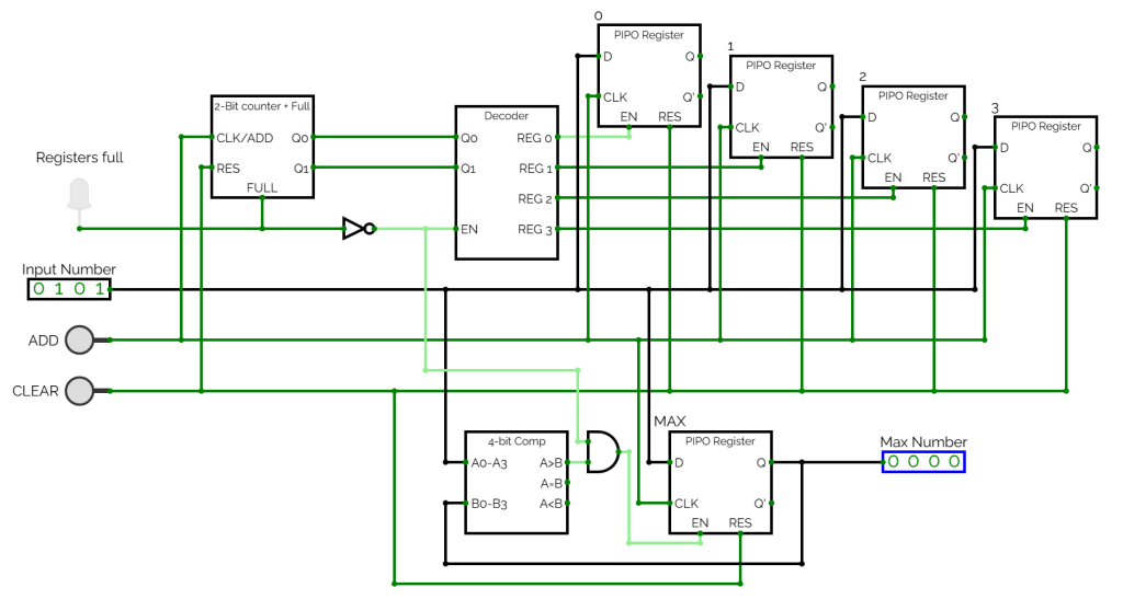
Circuit 4: register-based max finder (CircuitVerse simulation)
Four 4-bit registers store values as they arrive; a fifth register holds the running maximum across them. An ADD button commits the current DIP-switch input into the next available storage slot and, independently, updates the max register if the new value exceeds what’s already there. A CLEAR button resets every slot and the max. A FULL LED lights once all four storage slots are occupied and freezes further updates until CLEAR.
Open the CircuitVerse simulation →
Design narrative
Circuit 4 is Circuit 2’s sequential cousin — instead of comparing three inputs all present at the same instant, it stores four values as they arrive and keeps a running maximum across them. I had only planned to build the registers as a sub-circuit, but once I got going I couldn’t stop.
The build took a few turns. CircuitVerse doesn’t ship a 4-bit register as a single part, so each register became its own subcircuit — four D flip-flops sharing the same clock, enable, and reset signals. That was the first time I’d built a register from scratch. The 4-bit magnitude comparator started as a fork from a public CircuitVerse project, but its wiring was broken in ways that were faster to rebuild than to debug. Twelve gates do the per-bit compares, and thirteen more combine those into an overall greater-than / equal / less-than verdict — 25 gates total, wrapped as a subcircuit.
The bug I caught before submitting is one worth writing about. I ran three input patterns through the circuit: a series of increasing numbers, a series of decreasing numbers, and a large value after the storage registers were full. The first two worked. On the post-full spike, the max register kept updating even though the bank was supposed to have frozen. My first plan had a MUX in front of R_MAX — a small switch that would pick between ‘take the new input’ and ‘hold what you’ve got,’ driven by the comparator. Once I saw the bug, it was clear R_MAX also needed to freeze when FULL latched. The D flip-flops have an enable pin — a simple on/off for writes — and one AND gate on that pin did both jobs: only let R_MAX update when the new input is bigger, and only when the bank isn’t full. The MUX was no longer necessary, so it came out.
Inputs, outputs, and behavior
Inputs
- INPUT[3:0] — 4-bit unsigned value on DIP switches, range 0–15.
- ADD — pushbutton. Rising edge advances the fill counter, conditionally updates R_MAX, and (if not full) commits INPUT to the register pointed to by the counter.
- CLEAR — pushbutton. Asynchronous reset — clears all storage registers, R_MAX, the fill counter, and the FULL latch to zero.
Outputs
- R_MAX.Q[3:0] — 4 output probes, binary readout of the current maximum.
- FULL — 1 red LED. Lights HIGH when all four storage registers are occupied; cleared by CLEAR.
Behavior
- CLEAR pressed: All five PIPO registers, the fill counter, and the FULL latch asynchronously reset to 0.
- ADD pressed, FULL = 0: INPUT loads into the register pointed to by the fill counter (R0 if 00, R1 if 01, R2 if 10, R3 if 11). The counter advances, saturating at 11. Independently, if INPUT > R_MAX then R_MAX takes the new value; otherwise R_MAX holds.
- ADD pressed, FULL = 1: All LOAD lines are gated to 0 by NOT-FULL — no storage register loads. The counter stays at 11. R_MAX.EN is also gated by NOT-FULL, so R_MAX freezes even if a post-full INPUT exceeds the stored max. FULL stays HIGH until CLEAR.
Boolean expressions and truth tables
The register bank, the fill counter, the LOAD decoder, the FULL latch, and the R_MAX enable all come from a small set of expressions. Walking the data path from the register primitive outward:
PIPO register subcircuit
Each 4-bit register is a subcircuit built from four of CircuitVerse’s featured D flip-flops sharing the same CLK, EN, and asynchronous RES signals. D[3:0] enters through a splitter and fans out one line to each DFF’s D pin; Q[3:0] joins back out through a splitter on the opposite side. The featured DFF’s built-in EN pin carries the load-enable directly — no external 4-bit 2-to-1 mux was needed to choose between “load” and “hold.”
Fill counter — 2-bit saturating up-counter
Q0Q1 is both the count of filled registers and the pointer to the next register to fill. Next-state table:
| Q0 Q1 | Q0' Q1' |
|-------|---------|
|  0  0 |   0  1  |
|  0  1 |   1  0  |
|  1  0 |   1  1  |
|  1  1 |   1  1  |  (saturates)
Deriving the D inputs from the table and simplifying by absorption (A + A’B = A + B):
D0 = Q0'Q1 + Q0Q1' + Q0Q1
   = Q0'Q1 + Q0
   = Q0 + Q1

D1 = Q0'Q1' + Q0Q1' + Q0Q1
   = Q1' + Q0Q1
   = Q1' + Q0
2-to-4 LOAD decoder
The decoder turns the counter’s pointer into a single active LOAD line, gated by NOT FULL so that a post-full ADD can’t overwrite a stored value:
LOAD_R0 = NOT FULL · Q0' · Q1'
LOAD_R1 = NOT FULL · Q0' · Q1
LOAD_R2 = NOT FULL · Q0  · Q1'
LOAD_R3 = NOT FULL · Q0  · Q1
FULL latch
A separate D flip-flop clocked by ADD tracks whether the bank is full. Its D input is a single AND:
D_FULL = Q0 · Q1
On the ADD edge where Q0Q1 is already 11 (the edge that fills R3), D_FULL is 1, so FULL latches HIGH on that same edge. It stays HIGH until CLEAR.
The counter is doing two jobs at once, and that’s why the FULL flip-flop is a separate piece of state. It tracks which register is next to fill (Q0Q1 as a 2-bit pointer: 00→R0, 01→R1, 10→R2, 11→R3), and it has to tell the rest of the circuit whether any registers are still empty — because once they’re all full, new inputs have to bounce off. A combinational Q0·Q1 tap tries to do both off the same two bits, but it conflates “pointing at the last slot” with “all slots full” — it would assert FULL while R3 is being loaded, not after. The two questions need two pieces of state. My saturating counter can’t tick past 11 to signal “done” on its own, so the FULL flip-flop is the second piece: D_FULL = Q0·Q1 latches HIGH on the clock edge after the pointer lands on R3, so FULL reads “done loading” rather than “pointing at the last slot.”
After I submitted, feedback on the design pushed me further, and an alternative surfaced that I hadn’t seen during scoping. It handles the same two jobs with different hardware — keep the counter as the pointer, but derive “any registers still empty” combinationally from R_MAX instead of latching it in a flip-flop. Let the counter wrap (00 → 01 → 10 → 11 → 00) instead of saturating, and put the “bank still has room” logic outside the counter as an enable — ENABLE = Q0 + Q1 + Reg_MT, where Reg_MT is “some register is still empty.” That enable gates both the counter’s advance and every register’s load. The catch is where Reg_MT comes from. Source it from R_MAX by checking whether all four bits are zero and I save the whole flip-flop — but I also commit to calling an all-zero input stream “empty.” On random 4-bit inputs that misclassification rate is (1/16)⁴ ≈ 0.0015%. As I put it when I worked through this: if you’re checking four zeros against each other to see what’s biggest, you have bigger problems than the 0000 empty state.
The flip-flop savings aren’t free, though. Counting gates: the R_MAX zero-detect is a 4-input NOR, the enable needs a 3-input OR to fold in Q0 and Q1, and the counter needs ANDs on its D-paths so ENABLE = 0 freezes the advance. The FULL latch I shipped costs one AND (D_FULL = Q0·Q1) and one inverter for NOT FULL. So the alternative saves a flip-flop but spends a bunch of gates on the outside logic. I didn’t see this alternative until feedback pushed me to look for it — but even after working through it, I still think counter+FULL is the more elegant path.
R_MAX enable
R_MAX shares the INPUT bus with the four storage registers; its EN pin alone decides whether the current INPUT becomes the new max. One AND gate handles both the “new value is actually bigger” condition and the “bank is full, freeze everything” condition:
R_MAX.EN = NOT FULL · CMP_MAX.GT
| FULL | GT | EN | R_MAX behavior      |
|------|----|----|---------------------|
|   0  |  0 |  0 | hold (INPUT ≤ max) |
|   0  |  1 |  1 | load new max        |
|   1  |  0 |  0 | frozen (bank full)  |
|   1  |  1 |  0 | frozen (bank full)  |
The NOT-FULL half of this gate was added after the verification sweep caught R_MAX drifting past FULL on a post-full input spike.
Stretch (contingent on feedback)
- Display-on-demand. A LOAD button and a separate R_DISP register, so the current max reads out only when requested rather than continuously.
- Decimal display. GE10 detect + subtract-10 path feeding two 7447 decoders, for a two-digit seven-segment readout.
- 4-bit adder subcircuit. Required by the decimal-decode path.
Acknowledgment
Claude Opus 4.X (Anthropic) served as my thinking partner for the design and presentation of this project. It helped me brainstorm, organize my working notes, and draft the prose, tables, and diagrams on this page at my direction. All design decisions were mine, and all Boolean minimization and schematic work were done by hand or with purpose-built tools — not by Claude. I own the final work.
References
[1] A. J. Pasquale, Digital Systems. Self-published, rev. 2 Dec. 2025. Referenced throughout.
[2] 32×8: Boolean Minimization. Available: http://www.32×8.com. Referenced during planning; not used for this circuit — the CMP4 logic was hand-derived.
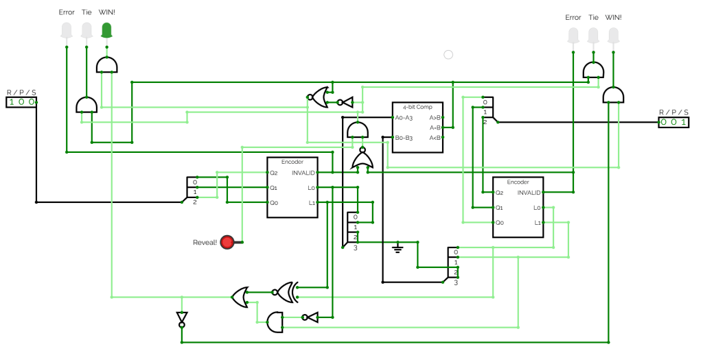
Circuit 5: Rock-Paper-Scissors judge (CircuitVerse simulation)
Two-player rock-paper-scissors judge. Each player picks Rock, Paper, or Scissors on a one-hot three-switch input; a reveal button gates the display; two common-cathode RGB LEDs signal per-player outcomes — green for a win, blue for a tie, red for an invalid input on that side. Purely combinational — no latching, no clocks.
Open the CircuitVerse simulation →
Design narrative
Circuit 5 is a two-player rock-paper-scissors judge. Each side enters a move on three labeled switches — R, P, S — and the circuit declares a winner, a tie, or an invalid input, driving a per-player RGB LED: green for a win, blue for a tie, red when that side’s input isn’t exactly one-hot. Out of 64 possible input combinations, nine are valid pairs; the remaining 55 are invalid on at least one side. The design ended up more interesting than I expected — a couple of things fell out of the minimization that I didn’t see coming.
I started wiring the three switches on each side straight through to the winner and tie logic. But then checking for invalid inputs was going to have to happen everywhere downstream — every expression would need to carry a “this side is legal” term, and the top-level logic would get cluttered. So I put a 3-to-2 validating encoder in front of each side to handle validity cleanly: it raises an error flag if the input isn’t exactly one-hot, and it hands the winner/tie logic a signal that’s already been vetted. Since the one-hot format was only there for the user at the switch panel — internal logic doesn’t care about the R/P/S labels — the encoder also drops the bus from 3 bits to 2 bits on its way through: R = 00, P = 01, S = 11, with 10 left as a gap in the codespace. From there, everything downstream operates on the 2-bit codes plus an E flag per player.
With the codes as 2-bit numbers, tie detection fell out of a 4-bit magnitude comparator: feed the two codes in as the A and B operands (upper two bits tied low) and the EQ output is the tie signal directly. No hand-built match network. For the winner logic, I took the four code bits plus the comparator’s A>B output into 32×8.com as a 5-variable minimization, with every tie row and every row where one or both sides are invalid marked as don’t-cares. Two things came out of that. First, the don’t-cares absorbed the A>B variable entirely — it drops out of the final expression, so the comparator’s A>B output is available but the winner function never uses it. Second, the minimized Awin came back as three terms, two of which factor into an XNOR, giving a compact expression.
Before running the minimization, I could already see from the rule table that the two winner outputs would be complements — under the “both valid, not tied” restriction, Awin’s maxterms are exactly Bwin’s minterms and vice versa, so NOT Awin = Bwin is forced by the rule table itself. I minimized both independently (SOP) on 32×8 to see which one was worth building. I was surprised at how different they were. Awin minimized the A>B term completely out of the expression and reduced to three 2-input gates. For Bwin, the A<B term stayed, and it factored but didn’t do anything especially cute and used 1 more gate and several more nots. So the build uses the minimized Awin with a single inverter on the output for Bwin — fewer gates than a parallel winner network, and the two outputs can’t drift out of sync during edits.
The first wiring had the cycle running backwards — Rock was beating Paper and losing to Scissors. Rather than re-deriving the winner expressions, the fix was to swap two of the one-hot switch wires at the encoder input on both encoders. The encoding assigns numerical codes (R=00, P=01, S=11), and which physical switch maps to which code decides whether the R → P → S cycle runs forward or backward. Four wires, two swaps, no minimization to redo.
The final stage is a priority chain at the LEDs. Reds come straight off the per-side error flags and aren’t gated by the reveal button — if a player enters an invalid move, they see their red immediately, while they’re still picking, not only after the button press. That way they know they’re ready to reveal when both red lights are off. Blues and greens go through a shared enable signal. I tied the button into the error-free signal right at that node, so the button rides along on the same enable that feeds every blue and green line. Just one gate instead of and-ing it into every line.
Inputs, outputs, and behavior
Inputs
- A_R, A_P, A_S — Player 1 move, one-hot. Exactly one high for a valid entry.
- B_R, B_P, B_S — Player 2 move, one-hot.
- button — momentary reveal enable. Held → blues and greens display; released → blues and greens go dark. Reds are not gated by the button.
Outputs
- P1_Red, P1_Green, P1_Blue — Player 1 side of a common-cathode RGB LED.
- P2_Red, P2_Green, P2_Blue — Player 2 side of a common-cathode RGB LED.
Per-side color semantics: green — this side wins the round; blue — tie (lights on both sides simultaneously); red — this side’s input is invalid.
Simulation representation. CircuitVerse’s RGB LED component expects 8-bit inputs per channel (intensity 0–255), which doesn’t match the 1-bit on/off signals from this circuit. The schematic uses three discrete LEDs per side (red, green, blue, tinted via the component color property), wired to the three per-side signals. This arrangement represents a common-cathode RGB LED as it would appear in a real build — the shared ground across the three channels corresponds to the common cathode pin.
Behavior
- Both sides valid, winner exists: the winning side’s green lights while the button is held; the other side is dark; no reds.
- Both sides valid, tie: both blues light while the button is held; no greens, no reds.
- One side invalid: that side’s red lights immediately (button state doesn’t matter); the other side is dark; no greens, no blues.
- Both sides invalid: both reds light; no greens, no blues.
- Button released: blues and greens dark. Reds unaffected.
Boolean expressions and truth tables
The circuit decomposes into four stages: the per-player validating encoder, the tie detector (the comparator’s EQ output), the winner cluster (minimized with don’t-cares), and the priority chain at the LED stage. Each stage’s expressions below.
3-to-2 validating encoder (per player)
Inputs: A_R, A_P, A_S (one-hot). Outputs: the 2-bit code AL0, AL1 (MSB first) and an error flag E_A. Encoding:
| Move   | AL0 AL1 | count of 1s |
|--------|---------|-------------|
|   R    |  0   0  |      0      |
|   P    |  0   1  |      1      |
|   S    |  1   1  |      2      |
|  (gap) |  1   0  |      —      |
By inspection:
AL0 = A_S                                (only S has MSB = 1)
AL1 = A_P + A_S                          (both P and S have LSB = 1)
E_A = NOT(exactly one of {A_R, A_P, A_S} is high)
Same structure for player B, producing BL0, BL1, E_B from B_R, B_P, B_S.
Rule table — nine valid rows
Rock crushes scissors. Paper covers rock. Scissors cut paper.
| P1 | P2 | A-code (AL0 AL1) | B-code (BL0 BL1) | Awin | Bwin | Tie |
|----|----|------------------|------------------|------|------|-----|
| R  | R  |      0   0       |      0   0       |   0  |   0  |  1  |
| R  | P  |      0   0       |      0   1       |   0  |   1  |  0  |
| R  | S  |      0   0       |      1   1       |   1  |   0  |  0  |
| P  | R  |      0   1       |      0   0       |   1  |   0  |  0  |
| P  | P  |      0   1       |      0   1       |   0  |   0  |  1  |
| P  | S  |      0   1       |      1   1       |   0  |   1  |  0  |
| S  | R  |      1   1       |      0   0       |   0  |   1  |  0  |
| S  | P  |      1   1       |      0   1       |   1  |   0  |  0  |
| S  | S  |      1   1       |      1   1       |   0  |   0  |  1  |
All 55 other input combinations set E_A = 1 or E_B = 1 (or both), and the priority chain at the LED stage suppresses the winner and tie outputs whenever either side is invalid.
Tie detection
Tie = EQ                     from a 4-bit magnitude comparator with
                             A = { 0, 0, AL0, AL1 }
                             B = { 0, 0, BL0, BL1 }
The upper two bits of each comparator operand are tied low (the codes are 2-bit), so EQ asserts exactly when the two codes match — the three tie rows in the rule table above.
Winner detection — 5-variable minimization with don’t-cares
Variables for the minimization: X (the comparator’s A>B output) and the four code bits AL0, AL1, BL0, BL1. Winner minterms enumerated from the rule table as 5-bit vectors X‑AL0‑AL1‑BL0‑BL1:
A winners:
  R beats S    X=0  A=00  B=11   →  00011  (3)
  P beats R    X=1  A=01  B=00   →  10100  (20)
  S beats P    X=1  A=11  B=01   →  11101  (29)

B winners:
  P beats R    X=0  A=00  B=01   →  00001  (1)
  S beats P    X=0  A=01  B=11   →  00111  (7)
  R beats S    X=1  A=11  B=00   →  11100  (28)
All nine tie rows plus all 55 rows with one or both sides invalid are marked as don’t-cares in the minimizer — the priority chain at the LED stage handles those cases. 32×8.com returns:
Awin = AL1'·BL0  +  AL0'·BL1'  +  AL1·BL1
     = AL1'·BL0  +  (AL0 XNOR BL1)
The AL0'·BL1' + AL1·BL1 pair factors to (AL0 XNOR BL1) after pulling out the common structure — verified by expanding the XNOR against the original three Awin minterms. Observation: the X variable drops out entirely. The comparator’s A>B output is available to the minimizer but doesn’t appear in the final expression — the don’t-cares subsume the need for it.
Bwin via a single inverter
Under the “both valid, not tied” restriction, the 3 Awin minterms and the 3 Bwin minterms partition the space — so Bwin = NOT Awin by definition over that restriction, before any minimization is run. Running De Morgan on the minimized Awin confirms it algebraically:
Awin      = AL1'·BL0  +  (AL0 XNOR BL1)
NOT Awin  = (AL1 + BL0')·(AL0 XOR BL1)        [De Morgan + XNOR negation]
          = Bwin
To decide which of the two to actually build, I minimized Bwin independently as SOP on 32×8.com. Unlike Awin, Bwin’s minimized SOP kept the A<B (comparator complement) term — the don’t-cares didn’t absorb it — and it didn’t factor into a clean XNOR the way Awin did. The gate count came in about one gate higher than Awin, with several more inverters. So the build uses the minimized Awin and hangs a single inverter on the output to produce Bwin — fewer gates than a parallel winner network, and the two outputs can’t drift out of sync during edits.
Priority chain at the LED stage
V        = NOR(E_A, E_B)             (both sides valid)
enable   = V · button                (single AND at the enable node)

P1_Red   = E_A                       (not button-gated)
P2_Red   = E_B                       (not button-gated)
P1_Blue  = EQ · enable               (both sides blue on a tie)
P2_Blue  = EQ · enable
P1_Green = Awin · EQ' · enable
P2_Green = Bwin · EQ' · enable
The EQ' term on the greens suppresses green-on-tie leakage; the enable term suppresses all blue and green output when the button is released or either side is invalid. Reds pass through directly from the encoder error flags, so a player sees their own invalid-input indication while still picking their move.
Architectural seam: the enable input
Everything upstream of the final enable AND — encoders, comparator, winner logic, and the LED priority chain — is combinational and doesn’t depend on how the enable signal is produced. That makes the reveal mechanism a swappable front end. Shape A (the build) uses enable = V · button. Shape B, documented as a stretch extension, swaps the button for a sequential one-shot that turns a press into a self-clearing pulse — the judge core is unchanged.
Stretch (future extension)
- Shape B — timed reveal wrapper. A sequential one-shot driven by the button edge; its output
reveal_activereplacesbuttoninenable = V · reveal_active. Tap once, see the outcome for a fixed window, auto-clears — instead of “hold to see the result.” - ROM-based rule lookup. The encoder output bus (two 2-bit codes plus two error flags) is a clean address-worth interface; a future CP3 ROM could replace the comparator and winner cluster with a lookup table without touching the input stage.
Acknowledgment
Claude Opus 4.X (Anthropic) served as my thinking partner for the design and presentation of this project. It helped me brainstorm, organize my working notes, and draft the prose, tables, and diagrams on this page at my direction. All design decisions were mine, and all Boolean minimization and schematic work were done by hand or with purpose-built tools — not by Claude. I own the final work.
References
[1] A. J. Pasquale, Digital Systems. Self-published, rev. 2 Dec. 2025. Referenced throughout.
[2] 32×8: Boolean Minimization. Available: http://www.32×8.com. Used for the 5-variable winner minimization with don’t-cares.
Circuit 1: signed 3-bit multiplier with signed, base 10, seven segment output
This circuit takes two 3-bit inputs A1A2A3 and B1B2B3 that are both 2’s complement values and multiplies them together. The output is formatted as a sign and magnitude value and displayed on three 7-segment displays. There is no overflow detection in this circuit, as all possible output values between negative 12 and positive 16 are capable of being displayed.
Click for the CircuitVerse Demo
Documentation
- Design Narrative
- 3-bit Multiplier Overview
- Hand written work sample
- LED decoding truth table
- Boolean expressions for lighting LED segments
- Selected K-Maps

Acknowledgment
Claude Opus 4.X (Anthropic) helped me draft this portfolio writeup. I own the final work.
Circuit 2: finds the largest of three 4-bit binary numbers and displays the largest value.
This circuit takes three 4-bit binary inputs X, Y and Z, and compares them, determining the largest. The largest value is displayed on two 7-segment displays. Three RGB LEDs (for X, Y and Z) show which of the numbers is largest with a green light. A red light indicates the number is the smallest of the three. Blue means the machine can’t determine the numbers relative magnitude.
Documentation
- Circuit Diagram
- Design Narrative
- Circuit 2 Truth tables
- L >= 10
- Base 10 Conversion for SevSeg LED
- Largest/Smallest/Unknown Indicator LEDs
Acknowledgment
Claude Opus 4.X (Anthropic) helped me draft this portfolio writeup. I own the final work.
